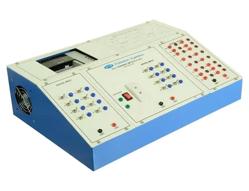
A PN junction diode apparatus is an essential educational equipment designed to provide students and learners with a clear understanding of the working principles and characteristics of a PN junction diode. Widely used in physics and electronics laboratories, this apparatus helps in studying the electrical behavior of a semiconductor diode under various conditions. Built with accuracy and reliability, it allows students to visualize and analyze the concept of forward and reverse bias, current-voltage characteristics, and the rectifying nature of a diode. This apparatus is a fundamental tool in electronics education, as the PN junction diode is considered the building block of modern semiconductor devices. By offering a practical platform for experimentation, it bridges the gap between theoretical concepts taught in textbooks and real-world electronic applications, ensuring effective learning outcomes for students in schools, colleges, and technical institutes.
Description
A PN junction diode apparatus is an educational electronics instrument designed to study the behavior of semiconductor diodes under different biasing conditions. It allows students to observe how a PN junction diode responds to forward and reverse bias. Because practical experimentation improves conceptual understanding, this apparatus helps learners analyze diode behavior and understand key semiconductor principles used in electronic circuits.
Key Features of PN Junction Diode Apparatus
- Mounted PN junction diode for experimentation
- Terminals for easy electrical connections
- Regulated power supply for controlled input
- Built-in meters for measuring voltage and current
- Supports forward and reverse bias experiments
- Enables plotting of diode V–I characteristics
Why Use
The PN junction diode apparatus allows students to apply forward and reverse bias to a diode and observe its electrical behavior. During experiments, learners measure parameters such as threshold voltage, knee voltage, and leakage current. Therefore, students can plot V–I characteristics and interpret the graphical behavior of semiconductor devices. This hands-on approach strengthens understanding of diode operation in real electronic circuits.
Applications of PN Junction Diode Apparatus
- Studying V–I characteristics of PN junction diodes
- Demonstrating forward and reverse bias behavior
- Understanding diode rectification in power supplies
- Exploring clipping and clamping circuits
- Teaching semiconductor fundamentals in electronics labs
Role of Apparatus in Research and Education
The PN junction diode apparatus helps students connect theoretical semiconductor concepts with practical circuit applications. It also introduces learners to advanced topics such as Zener regulation, transistor operation, and electronic switching circuits. Because the apparatus is designed with durable components and a user-friendly layout, it supports safe and effective experimentation in laboratories. As a result, it becomes an essential teaching tool in electronics and electrical engineering education.
For related laboratory and educational equipment, you may explore:
https://www.aseducationalkits.com/products-category/physics-lab-equipment/
For a broader range of laboratory and analytical solutions, professionals can also refer to:
https://interlabs.in/products-catalogue/


